Testing Capability
Kehuite laboratory operates in compliance with CNAS-CL01:2018 "General Requirements for the Competence of Testing and Calibration Laboratories" (ISO/IEC 17025:2017), the application guidelines for electrical testing, as well as international, national, and industry standard methodologies. Upholding the principles of fairness, impartiality, scientific rigor, and efficiency, the testing center provides reliable and professional inspection services to clients.
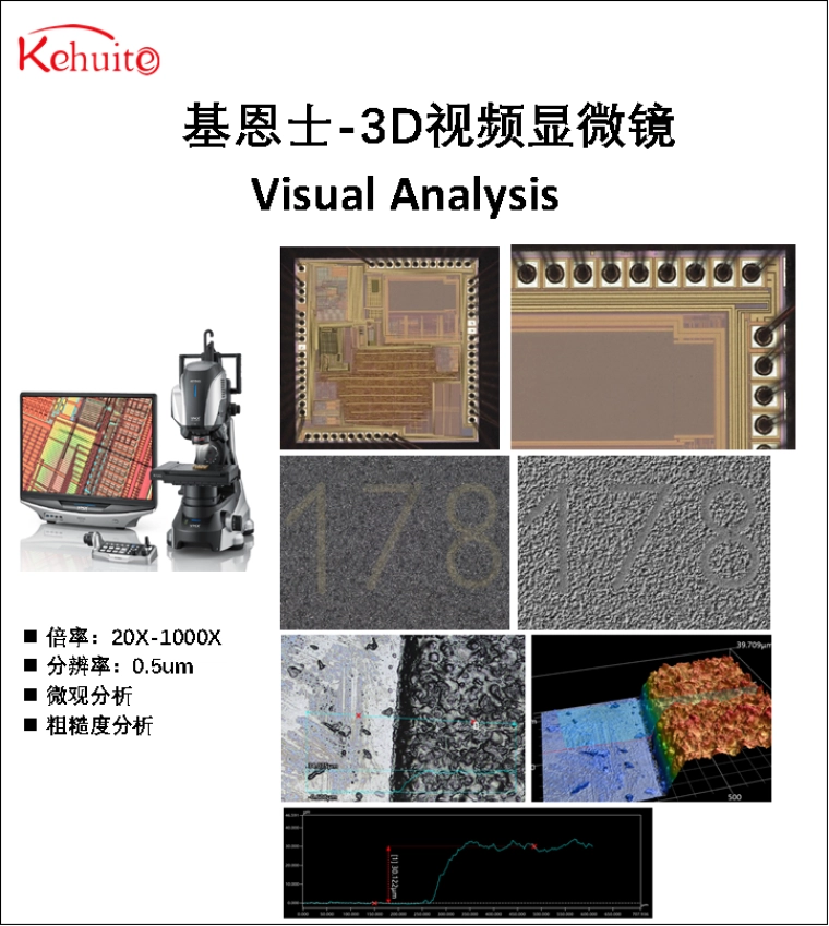
The main testing equipment includes: Keyence 3D ultra-deep field microscope, X-ray inspection system, chemical lid opening equipment, solderability testing equipment, video microscope, high and low temperature test chamber, electrical testing equipment, etc.
Our main inspection scope includes: the appearance, size, solderability, chip cover opening, functional inspection, reliability inspection, chip authenticity identification and device-level failure analysis of electronic components, etc.
Visual Analysis:
External Visual Inspection refers to verifying whether the received goods meet the requirements in terms of internal and external packaging, labeling information on the packaging, chip carriers, and moisture-sensitive protection.
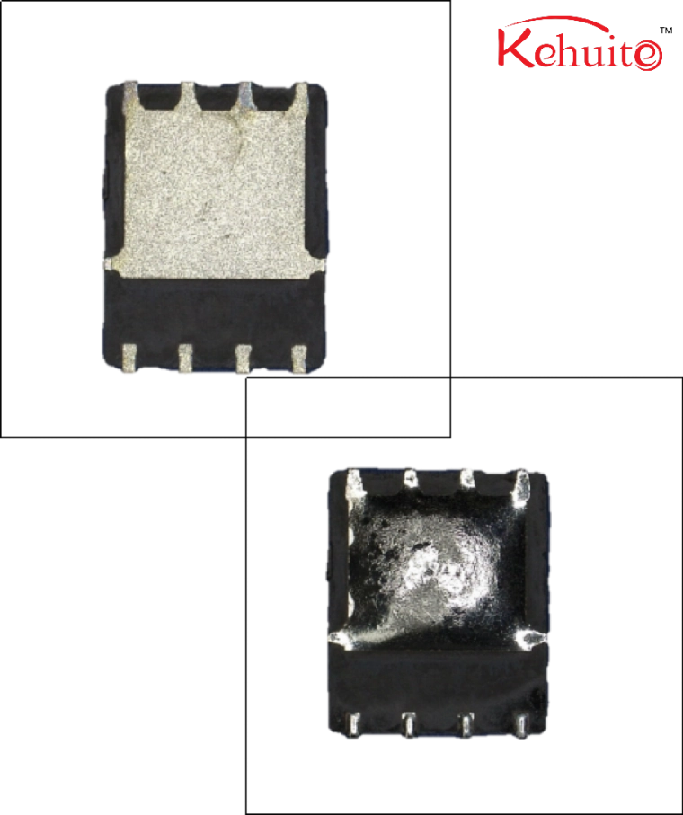
Subsequently, an individual chip undergoes an appearance inspection, which mainly includes:
1. Checking whether the chip surface texture is uniform
2. Verifying if the markings are clear and the font is consistent
3. Inspecting the surface for signs of polishing or recoating
4. Examining the pins for defects such as re-tinning, deformation, oxidation, scratches, etc.
Scope of application:
According to relevant testing standards, determine whether the chip is brand new, refurbished, and whether the pins are tinned or oxidized, etc.
Applicable standard:
1. Counterfeit and Substandard Product Detection Procedure
2. Electronic Component Testing Methods and Procedures
3. U.S. Military Standard
Solvent Testing (DY750 solvent Testing):
This test includes mark permanency testing (applicable only to inkjet-printed markings), acetone testing, and HCT (Hot Chemical Test).
Through the corrosive action of chemical reagents, it removes surface coatings and silkscreen printing from the chip to verify whether the chip exhibits signs of: Grinding marks, Recoating, Remarking (reprinted text).
The test helps detect potential counterfeit or refurbished components by exposing surface alterations.
Scope of application:
It is typically performed alongside visual inspection to help identify and eliminate refurbished/counterfeit components.
Applicable standard:
AS6171-2A
AS6081
.webp)
.webp)
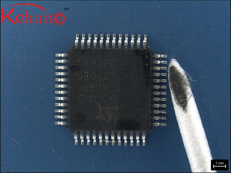
Acetone Testing:
Acetone testing involves using a cotton swab dipped in a certain concentration of acetone to regularly wipe the front surface of the chip ten times. Determine whether the chip surface shows signs of refurbishment based on whether the cotton swab turns black.
Scope of application:
It is typically performed alongside visual inspection to help identify and eliminate refurbished/counterfeit components.
Applicable standard:
AS6171-2A
AS6081
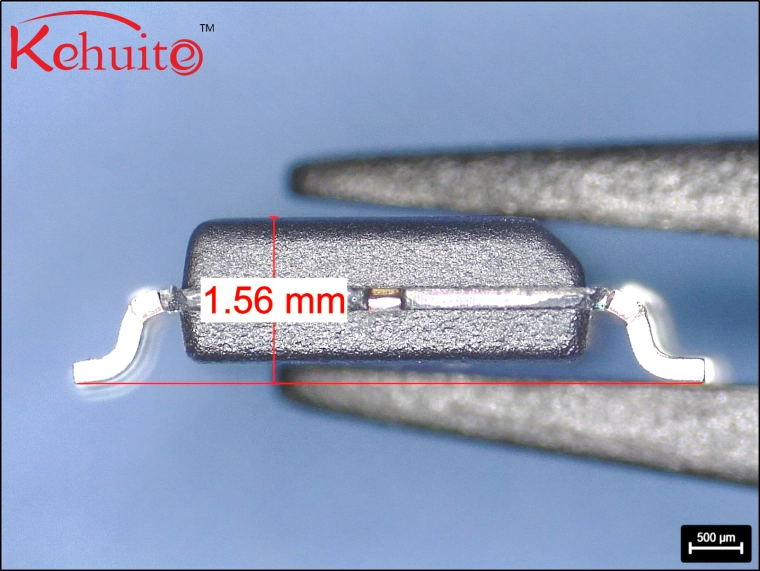
Dimensional Testing:
Dimensional testing is to measure the external dimensions of the sample according to the dimensional requirements in the sample specification sheet, and verify whether there are issues such as grinding and re-coating on the chip surface through dimensional comparison.
Scope of application:
It is usually combined with appearance inspection to verify and rule out refurbished goods.
Applicable standard:
AS6171-2A
AS6081
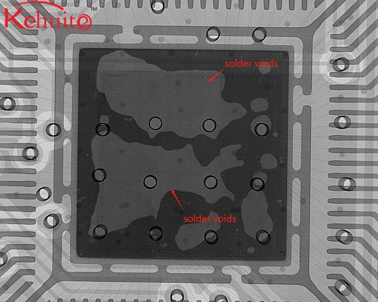
X-ray Inspection:
X-ray inspection is a real-time, non-destructive analytical method applicable to consumer-grade, industrial-grade, and automotive-grade chips, as well as soldered assemblies. It is primarily used to examine the internal components of chip packaging, including wafer, bonding wire, substrate, adhesive and plastic packaging. It can also detect various abnormalities such as wafer cracks, voids in adhesives, adhesive fillet height, wire arc, foreign matter in molding compound, tilting and soldering of internal components in the module, ESD damage, etc. Moreover it can detect the internal consistency between original/genuine samples and ordinary samples.
Scope of application:
1.Defect detection (e.g., cracks, foreign objects) in metal materials & components, plastic materials & components, electronic components, electronic assemblies, and LED elements.
2.Internal displacement analysis of BGA (Ball Grid Array), PCBs (Printed Circuit Boards), etc.
3.Identification of soldering defects such as voids, cold soldering, and poor wetting in BGA joints.
Applicable standard:
AS6171-5 (Radioactive Detection Method)
GJB-548C (Electronic Component Testing Methods and Procedures)
MIL-STD-883L (U.S. Military Standard)
Solderability Testing:
Solderability testing is performed to verify that component leads and terminations satisfy standard-defined solderability criteria and to ensure that storage has no adverse effect on the component soldering onto the interconnection substrate.
Scope of application:
Solderability can be assessed during manufacturing, upon customer receipt of components, or before assembly and soldering.
Applicable standard:
J-STD-002E (Solderability tests for component leads, solder ends, tabs, terminals, and conductors)
MIL-STD-883L (U.S. Military Standard)